- 您现在的位置:买卖IC网 > Sheet目录2006 > LTC2492IDE#TRPBF (Linear Technology)IC ADC 24BIT DELTA SIG 14-DFN
LTC2492
31
2492fd
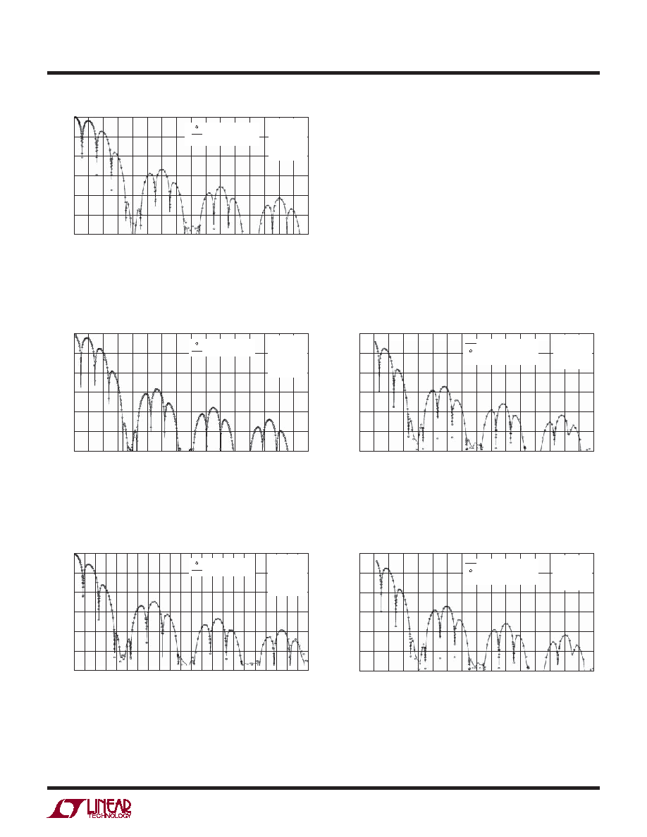
Figure 22. Input Normal Mode Rejection vs Input Frequency with
Input Perturbation of 100% (60Hz Notch)
APPLICATIONS INFORMATION
Traditional high order delta-sigma modulators suffer from
potential instabilities at large input signal levels. The
proprietary architecture used for the LTC2492 third order
modulator resolves this problem and guarantees stability
with input signals 150% of full-scale. In many industrial
applications, it is not uncommon to have microvolt level
signals superimposed over unwanted error sources with
several volts of peak-to-peak noise. Figures 25 and 26
show measurement results for the rejection of a 7.5V
peak-to-peak noise source (150% of full scale) applied
to the LTC2492. From these curves, it is shown that the
rejection performance is maintained even in extremely
noisy environments.
INPUT FREQUENCY (Hz)
0
15
30
45
60
75
90
105 120 135 150 165 180 195 210 225 240
NORMAL
MODE
REJECTION
(dB)
2492 F22
0
–20
–40
–60
–80
–100
–120
VCC = 5V
VREF = 5V
VIN(CM) = 2.5V
VIN(P-P) = 5V
TA = 25°C
MEASURED DATA
CALCULATED DATA
INPUT FREQUENCY (Hz)
0
12.5
25
37.5
50
62.5
75
87.5 100 112.5 125 137.5 150 162.5 175 187.5 200
NORMAL
MODE
REJECTION
(dB)
2492 F23
0
–20
–40
–60
–80
–100
–120
VCC = 5V
VREF = 5V
VIN(CM) = 2.5V
VIN(P-P) = 5V
TA = 25°C
MEASURED DATA
CALCULATED DATA
Figure 23. Input Normal Mode Rejection vs Input Frequency with
Input Perturbation of 100% (50Hz Notch)
INPUT FREQUENCY (Hz)
0
20
40
60
80
100
120
140
160
180
200
220
NORMAL
MODE
REJECTION
(dB)
2492 F24
0
–20
–40
–60
–80
–100
–120
VCC = 5V
VREF = 5V
VIN(CM) = 2.5V
VIN(P-P) = 5V
TA = 25°C
MEASURED DATA
CALCULATED DATA
Figure 24. Input Normal Mode Rejection vs Input Frequency with
Input Perturbation of 100% (50Hz/60Hz Notch)
INPUT FREQUENCY (Hz)
0
15
30
45
60
75
90
105 120 135 150 165 180 195 210 225 240
NORMAL
MODE
REJECTION
(dB)
2492 F25
0
–20
–40
–60
–80
–100
–120
VCC = 5V
VREF = 5V
VIN(CM) = 2.5V
TA = 25°C
VIN(P-P) = 5V
VIN(P-P) = 7.5V
(150% OF FULL SCALE)
Figure 25. Measure Input Normal Mode Rejection vs Input
Frequency with Input Perturbation of 150% (60Hz Notch)
INPUT FREQUENCY (Hz)
0
NORMAL
MODE
REJECTION
(dB)
2492 F26
0
–20
–40
–60
–80
–100
–120
VCC = 5V
VREF = 5V
VIN(CM) = 2.5V
TA = 25°C
VIN(P-P) = 5V
VIN(P-P) = 7.5V
(150% OF FULL SCALE)
12.5
25
37.5
50
62.5
75
87.5 100 112.5 125 137.5 150 162.5 175 187.5 200
Figure 26. Measure Input Normal Mode Rejection vs Input
Frequency with input Perturbation of 150% (50Hz Notch)
发布紧急采购,3分钟左右您将得到回复。
相关PDF资料
LTC2493IDE#TRPBF
IC ADC 24BIT DELTA SIG 14-DFN
LTC2494IUHF#TRPBF
IC ADC 16BIT W/PGA 38-QFN
LTC2495CUHF#PBF
IC ADC 16BIT W/PGA 38-QFN
LTC2496IUHF#TRPBF
IC ADC 16BIT DELTA SIG 38-QFN
LTC2498IUHF#TRPBF
IC ADC 24BIT 16CH 38-QFN
LTC2600IUFD#PBF
IC DAC OCTAL R-R 16BIT 20-QFN
LTC2602IMS8#TRPBF
IC DAC 16BIT DUAL R-R VOUT 8MSOP
LTC2604IGN-1#TRPBF
IC DAC 16BIT QUAD R-R OUT 16SSOP
相关代理商/技术参数
LTC2493CDE#PBF
功能描述:IC ADC 24BIT DELTA SIG 14-DFN RoHS:是 类别:集成电路 (IC) >> 数据采集 - 模数转换器 系列:- 标准包装:2,500 系列:- 位数:16 采样率(每秒):15 数据接口:MICROWIRE?,串行,SPI? 转换器数目:1 功率耗散(最大):480µW 电压电源:单电源 工作温度:-40°C ~ 85°C 安装类型:表面贴装 封装/外壳:38-WFQFN 裸露焊盘 供应商设备封装:38-QFN(5x7) 包装:带卷 (TR) 输入数目和类型:16 个单端,双极;8 个差分,双极 配用:DC1011A-C-ND - BOARD DELTA SIGMA ADC LTC2494
LTC2493CDE#TRPBF
功能描述:IC ADC 24BIT DELTA SIG 14-DFN RoHS:是 类别:集成电路 (IC) >> 数据采集 - 模数转换器 系列:- 标准包装:2,500 系列:- 位数:16 采样率(每秒):15 数据接口:MICROWIRE?,串行,SPI? 转换器数目:1 功率耗散(最大):480µW 电压电源:单电源 工作温度:-40°C ~ 85°C 安装类型:表面贴装 封装/外壳:38-WFQFN 裸露焊盘 供应商设备封装:38-QFN(5x7) 包装:带卷 (TR) 输入数目和类型:16 个单端,双极;8 个差分,双极 配用:DC1011A-C-ND - BOARD DELTA SIGMA ADC LTC2494
LTC2493CDEPBF
制造商:Linear Technology 功能描述:24bit Delta Sigma ADC Temp Sens LTC2493
LTC2493IDE#PBF
功能描述:IC ADC 24BIT DELTA SIG 14-DFN RoHS:是 类别:集成电路 (IC) >> 数据采集 - 模数转换器 系列:- 标准包装:1 系列:microPOWER™ 位数:8 采样率(每秒):1M 数据接口:串行,SPI? 转换器数目:1 功率耗散(最大):- 电压电源:模拟和数字 工作温度:-40°C ~ 125°C 安装类型:表面贴装 封装/外壳:24-VFQFN 裸露焊盘 供应商设备封装:24-VQFN 裸露焊盘(4x4) 包装:Digi-Reel® 输入数目和类型:8 个单端,单极 产品目录页面:892 (CN2011-ZH PDF) 其它名称:296-25851-6
LTC2493IDE#TRPBF
功能描述:IC ADC 24BIT DELTA SIG 14-DFN RoHS:是 类别:集成电路 (IC) >> 数据采集 - 模数转换器 系列:- 标准包装:1,000 系列:- 位数:16 采样率(每秒):45k 数据接口:串行 转换器数目:2 功率耗散(最大):315mW 电压电源:模拟和数字 工作温度:0°C ~ 70°C 安装类型:表面贴装 封装/外壳:28-SOIC(0.295",7.50mm 宽) 供应商设备封装:28-SOIC W 包装:带卷 (TR) 输入数目和类型:2 个单端,单极
LTC2494CUHF#PBF
功能描述:IC ADC 16BIT W/PGA 38-QFN RoHS:是 类别:集成电路 (IC) >> 数据采集 - 模数转换器 系列:- 标准包装:2,500 系列:- 位数:16 采样率(每秒):15 数据接口:MICROWIRE?,串行,SPI? 转换器数目:1 功率耗散(最大):480µW 电压电源:单电源 工作温度:-40°C ~ 85°C 安装类型:表面贴装 封装/外壳:38-WFQFN 裸露焊盘 供应商设备封装:38-QFN(5x7) 包装:带卷 (TR) 输入数目和类型:16 个单端,双极;8 个差分,双极 配用:DC1011A-C-ND - BOARD DELTA SIGMA ADC LTC2494
LTC2494CUHF#TRPBF
功能描述:IC ADC 16BIT W/PGA 38-QFN RoHS:是 类别:集成电路 (IC) >> 数据采集 - 模数转换器 系列:- 标准包装:2,500 系列:- 位数:16 采样率(每秒):15 数据接口:MICROWIRE?,串行,SPI? 转换器数目:1 功率耗散(最大):480µW 电压电源:单电源 工作温度:-40°C ~ 85°C 安装类型:表面贴装 封装/外壳:38-WFQFN 裸露焊盘 供应商设备封装:38-QFN(5x7) 包装:带卷 (TR) 输入数目和类型:16 个单端,双极;8 个差分,双极 配用:DC1011A-C-ND - BOARD DELTA SIGMA ADC LTC2494
LTC2494IUHF#PBF
功能描述:IC ADC 16BIT W/PGA 38-QFN RoHS:是 类别:集成电路 (IC) >> 数据采集 - 模数转换器 系列:- 标准包装:1 系列:microPOWER™ 位数:8 采样率(每秒):1M 数据接口:串行,SPI? 转换器数目:1 功率耗散(最大):- 电压电源:模拟和数字 工作温度:-40°C ~ 125°C 安装类型:表面贴装 封装/外壳:24-VFQFN 裸露焊盘 供应商设备封装:24-VQFN 裸露焊盘(4x4) 包装:Digi-Reel® 输入数目和类型:8 个单端,单极 产品目录页面:892 (CN2011-ZH PDF) 其它名称:296-25851-6